Definitions
| Oscilátors types | Definitions |
|---|---|
| CXO ( PXO, MXO ) | Single crystal oscillator, has frequency stability of the crystal units |
| VCXO | Voltage controlled crystal oscillators, can change the oscillation frequency with external voltage |
| TCXO | Temperature compensated crystal oscillator, compensated for frequency changes caused by the external temperature |
| OCXO | Oven control crystal oscillator, includes a temperature stabilized resonator |
| Term | Unit | Definitions |
|---|---|---|
| Nominal frequency fo ( Output frequency ) |
[MHz] | Nominal value of the frequency described in specifications. It is the output frequency at the standard temperature (usually 25oC), specified power supply voltage and load. |
| Frequency stability | [ppm] | The frequency range before and after specific ambient conditions such as temperature, power supply input variations, load variations, operation time (aging, long-term stability), etc. |
| Aging ( Long-term stability ) |
[ppm/year] | The frequency deviation with the lapse of time during normal operation |
| Frequency stability vs. supply voltage |
[ppm/V] | Frequency deviation when the power supply input voltage is varied. |
| Frequency stability vs. mechanical environment | [ppm] | Specified by the deviation before and after shock, dropping, sine wave vibration, constant acceleration, etc. applied. |
| Frequency stability vs. load |
[ppm] / Z | Frequency deviation when the load conditions have varied from the standard value. |
| Operation temperature range |
[ °C ] | The temperature range which the oscillator can safely operate. The frequency tolerance cannot be maintained outside the specified limits. |
| Storage temperature range |
[ °C ] | Maximum absolute temperatures allowed in the discharged state. Exposure to temperatures outside these limits may result in damage. |
| Supply voltage | [ V ] | The DC input voltage necessary for oscillator operation. |
| Input current | [ mA ] | The amount of current consumption by an oscillator from the power supply. |
| Deviation (for VCXO type) |
[ V ] | This range indicates the width of output frequency that can be adjusted by control voltage. |
| Start-Up time | [msec], [sec] |
The specified time from oscillator power-up to the time the oscillator reaches steady state oscillation. |
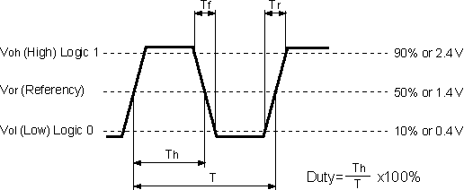
| Logic levels | [ 0, 1 ] | Defined as the Output Voltage Logic High or “Logic 1” and the Output Voltage Logic Low or “Logic 0”. |
| Rise time ( Tr ) | [ µs ] | The time taken for the output waveform to change from the low voltage level to the high voltage level. |
| Fall time ( Tf ) | [ µs ] | The time taken for the output waveform to change from the high voltage level to the low voltage level. |
| Duty cycle ( symmetry ) |
[ % ] | Measured at +1.4V for TTL oscillators and ½ Vdd level for universal, HCMOS and CMOS oscillators, this is the ratio of full and half cycles. |
| Internal Trim | This range indicates the width of frequency that can be adjusted by a trimmer built in the oscillator. |
|
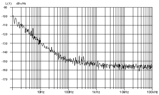
| Phase noise | The frequency domain measure of short term frequency stability of an oscillator. | |
| Short term stability | The random fluctuations of the frequency of an oscillator over short periods of time. |
- Cliped Sine
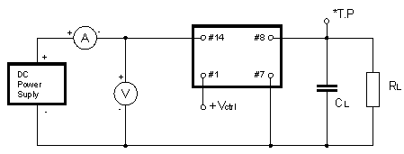
CL = 10 pF (including fixture and probe capacitances)
RL = 10
kΩ
RL = 10
kΩ
- CMOS
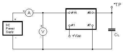
CL = 10 pF (including fixture and probe capacitances)
- TTL
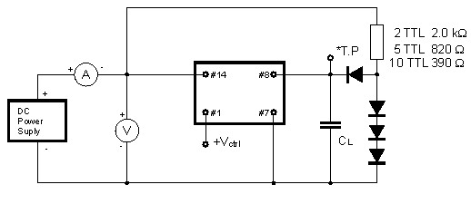
CL = 15 pF max (including fixture and probe capacitances)
*T.P = Test Point
*T.P = Test Point
- Output waveform
- Phase noise
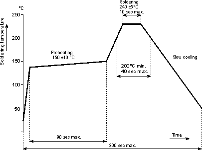
- REFLOW diagram