Warefs, substrates for SAW
Wafers are thin plates made of synthetic quartz with piezoelectric properties. These are starting product for production of devices on the base of surface acoustic wave (SAW).
We standardly produce wafers with diameters of 3 ”(76.2 mm) and 4“ (100.0 mm). According to customer requirements, respectively a particular application, we supply wafers with various surface qualities – from fine-lapped to polished with SAW quality. As a starting material in addition to the synthetic quartz can be used other piezoelectric crystalline materials such as lithium niobium (LN, LiNbO3), lithium tantalum (LT, LiTaO3) langasit (La3Ga5SiO14) and others.
We standardly produce wafers with diameters of 3 ”(76.2 mm) and 4“ (100.0 mm). According to customer requirements, respectively a particular application, we supply wafers with various surface qualities – from fine-lapped to polished with SAW quality. As a starting material in addition to the synthetic quartz can be used other piezoelectric crystalline materials such as lithium niobium (LN, LiNbO3), lithium tantalum (LT, LiTaO3) langasit (La3Ga5SiO14) and others.
Wafers are used for a wide range of applications, such as
– Components of SAW for the frequency stabilization and filtration (resonators, filters, oscillators)
– Components for sensors with SAW
– Optoelectronic components
– RF Microwave Circuits
– Biotechnic fields
– photolithography technology
etc.
Typical specifications of Quartz Wafers
| Parameter | 3″ substrate | 4″ substrate | tolerance |
|---|---|---|---|
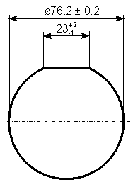
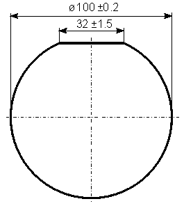
| Diameter [ mm ] | 76.2 | 100.0 | ±0.2 mm |
| Thickness [ µm ] | from 350 to 2000 µm, standard 350 or 500, resp. according to customer specification |
±10 µm | |
| Cut angle | family of ST cuts (rotated Y-cut around the X axis about 25° – 50°), cuts Y90°, Z90°, X90°, ZX 1°50‘, … special cuts according to customer specification |
±5\’ | |
| Cut angle marking | with slots on the main flat, and/or on side of the wafer, by using sec.flats – the size and location by customer, laser description below the primary flat – by customer specification |
||
|
The main flat – location
– length [mm] |
normally perpendicular to the axis-X 23 mm (3“) or 32 mm (4“) or customer specified |
±15\’ ±2 mm |
|
| Surface Quality | fine lapped- typically the back side – Ra = 0,12 – 0,20 µm, optically polished – Ra < 10 nm, polished SAW quality – RMS < 1 nm (different quality for each side can be choosen ) |
||
| TTV [ µm ] | < 8 | ||
| Bow [ µm ] | < 40 | ||
Specifications of synthetic quartz (according to EN/IEC 60758:2004, Ed.3 ):
|
grade C ( > 1.8 x 10⁶ ) grade Ib grade 3 |
Differences from standard values and other parameters can be consulted.
Reference
For more information about the quartz crystal can be obtained from the following technical standard:
EN (ISO) 60 758, Synthetic quartz crystal – Specifications and guidelines for use
Typical specifications of Quartz Wafers (Single Side Polished SAW)
| Parameter | 3-inch wafer | 4-inch wafer |
|---|---|---|
| Diameter (mm) | 76.2 ± 0.2 | 100.0 ± 0.2 |
| Thickness (µm) | standard 500 or 350 or customer specified | |
| Cut angle | family of ST-cuts with tolerance ± 5\’ | |
| LTV (µm) | better than 3 on the mesh 10 x 10 mm | |
| Bow (µm) | better than 40 | |
| Polished surface | SAW-quality, RMS better than 0.5 nm | |
| X-axis marking | by the flat (see drawing) or customer specified | |
Typical specifications of Langasite Wafers (Single Side Polished SAW)
| Parameter | 3-inch wafer | 4-inch wafer |
|---|---|---|
| Diameter (mm) | 76.2 ± 0.2 | 100.0 ± 0.2 |
| Thickness (µm) | standard 500 or 350 or customer specified | |
| Cut angle (Euler) | 0/65/0 deg, 0/90/0 deg, 0/26/35 deg, 0/138.5/26.7 deg with tolerance ± 6\’ |
|
| LTV (µm) | better than 8 on the mesh 10 x 10 mm | |
| Bow (µm) | better than 40 | |
| Polished surface | SAW-quality, RMS better than 0.7 nm | |
| X-axis marking | by the main and secondary flat | |
Outline dimensions [ mm ]
| 3″ wafer | 4″ wafer |
 |
 |